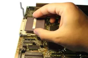
 Like a box of Lego bricks, field-programmable gate arrays (FPGAs) contain an array of programmable logic blocks designed to be configured after manufacturing, allowing the blocks to be intertwined in different configurations.
Modern FPGAs are very capable units that combine FPGA fabric with other components, such as microprocessor cores and various peripherals. Infinitely configurable FPGA fabric allows an electrical engineer to design an FPGA to perform virtually any function. In addition to the flexibility afforded by FPGA fabric, FPGA throughput is extremely high because of the parallel nature of an FPGA’s design.
Cardinal Peak’s Experience with FPGA Design
For the curious reader, we have included more details on how FPGAs work and how they are “programmed” following this brief summary of Cardinal Peak’s experience with FPGA design.
Cardinal Peak has several EEs skilled in FPGA implementation. Given Colorado’s strong aerospace market, many of our FPGA projects are for space contractors, although we do see commercial applications too. With the sensitive nature of most aerospace work, we cannot detail those projects in case studies, so below is a short, anonymized list of some representative projects we have recently completed that utilized FPGAs.
- Tasked with providing a high-speed, ultra-low-latency wireless link that demanded more than any off-the-shelf radio could provide, we opted to develop a custom modem implemented in programmable logic. We mated a Xilinx Zynq processor with an Analog Devices transceiver, enabling us to build a powerful, frequency-agile radio capable of meeting the application’s extreme requirements (sub-ms latency for sustained bi-directional 10 channel audio). Building the modem entirely in the FPGA fabric offered the speed and reliability of a dedicated ASIC with the flexibility to design a perfectly tailored solution to meet the customer’s needs.
- Utilizing a Xilinx Kintex FPGA we designed a multi-node, networked, digital signal processing system used for non-destructive testing. We also supported and improved upon legacy products needing additional functionality and fixes. These systems function similar to both active and passive doppler radar, by measuring arrival time/intensity of pulses received at multiple transducer points and cross-correlate channels to infer the location of defects in the vessel or the presence of water droplets within the vessel. This was an excellent application for FPGAs as the manufacturing volume is low, and the application required very high-speed measurement and processing in parallel.
- We have worked with several Pro-audio customers. One such design was a PCIe based Dante® networked audio system controller card. This design featured multiple Xilinx Spartan 6 and Artix 7 FPGAs. Critical to this design was an RTL architected to be capable of high bandwidth throughput, for which the FPGA is ideally suited. Additionally, we were required to optimize the Linux kernel, on the computer hardware (PC), to guarantee it would be able to keep up with the hardware.
- For another Pro-Audio customer, we were approached for a cost-reduction “re-design” of one of their network-centric digital signal and control processor lines, supporting over 400 bidirectional audio channels. The original Power-PC based design was re-architected using a Xilinx Artix-7 as a central router and variable number of Analog Devices DSPs for various product model configurations and options.
- We continue to work with several Aerospace clients. Their needs vary and, due to security, we do not detail what we do for them. What we can say is, most involve quite large Xilinx Kintex and UltraScale FPGAs used for terrestrial and flight systems. These are predominantly image processing applications involving extremely high speed “fat” data pipes (PCIe, Rapid-IO, Aurora, etc.), using DMA, and low-latency processing.
While most of our FPGA projects end up using Xilinx components, we occasionally develop using Altera (now Intel Agilex), Microsemi Libero, and Honeywell parts. Our team is well versed in both Xilinx and Altera (Intel) design and verification tools such as Vivado and Questa-sim.
If you need help developing a product that includes an FPGA, please reach out to us. We would be happy to provide our perspective in an initial conversation and tell you what your best options are.
With a focus on ultralow-latency communications and high-speed digital signal processing, our team leverages advanced FPGA technology to deliver customized, high-performance solutions that meet complex requirements across aerospace, pro audio and more.
FPGA Primer
For the curious reader, below is primer on FPGA and how they are programmed. Additionally, you may enjoy our Blog which provides a historical perspective on FPGA.
What is an FPGA?
An FPGA is a large array of primitive logic elements, such as memories, flip-flops and combinatorial logic (such as AND gates, OR gates, XOR gates and INVERTERs) all laid out in a huge matrix. The output of every logic element can be connected to the inputs of many other logic elements in such a way that any digital circuit function can be implemented within the limitations of the quantity and type of each logic element available.
These digital functions include but are not limited to state machines, counters, timers and digital signal processing engines. They can even be used to implement rudimentary central processing units (CPUs), although this is somewhat pointless because the biggest and most widely featured FPGAs include multiple CPUs built directly onto the silicon. As such, the FPGA acts not only as your custom logic but also as your embedded CPU.
The confusing-but-simple method by which the output of any logic element can be connected to the inputs of many other logic elements involves simply enabling the connection using a “1” stored in a nearby SRAM element that’s connected to an AND gate, which is located in series with the connection.
The many 1s programmed into the massive array of SRAMs (one for each possible connection) are usually through a serial interface in the FPGA and usually come from a reprogrammable EEPROM located nearby the FPGA. The FPGA then copies the binary file out of the EEPROM and into the FPGA to program itself upon every power-up.
As you can imagine, reprogramming the EEPROM — and having the FPGA reboot itself from the new EEPROM contents — allows for almost unlimited different digital circuit functions to be implemented one at a time. This, in turn, allows for the possibility of upgrading the FPGA functionality in the field, after the customer has purchased the product. (Of course, this field-upgrade use case also opens up your product to the risk of hacking, but FPGA development tools offer features that can be used to authenticate the origin of such an image file in order to prohibit configuring the FPGA from unauthorized image files.)
What is an FPGA Well Suited For?
 FPGAs are well suited for implementing any mostly digital circuit that is running at very high clock rates for any industry segment that does not have the volume to warrant the outrageous cost of developing an application-specific integrated circuit (ASIC). FPGAs are well suited for test and measurement, avionics, aerospace, infotainment, set-top boxes and more. Except for extremely high-volume consumer electronics, such as cell phones and laptops, FPGAs are in most electronics.
They are especially well suited for high-speed acceleration of CPU algorithms (such as digital signal processing algorithms), which are reimplemented in highly parallelized digital “fabric,” implementing the algorithms much faster than would be possible with a traditional CPU architecture.
Higher-end FPGAs also come with advanced CPUs, ADCs, DACs, UARTs, I2C, SPI, I2S, DRAM controllers, Ethernet physical layer (PHY) transceivers and other high-performance embedded processor features. This allows many embedded products to be completely reimplemented in a single FPGA.
What Skills are Needed to Design FPGAs?
Each FPGA vendor provides a CAD tool suite to be used in developing the FPGA’s functionality, simulating the functionality and optimizing the performance.
Using the provided CAD tool (which can be somewhat expensive depending on the type and complexity of FPGA), the user can simply provide schematics drawn within the CAD tool, using a primitive library provided inside the CAD tool, to represent the intended functionality. This approach is seldom used today because schematics cannot scale effectively to the complexity required by today’s FPGA designs.
Instead, most FPGA developers utilize a hardware description language (HDL), such as the Very High-Speed Integrated Circuit hardware description language (VHSIC-HDL or just VHDL) or Verilog, which is a portmanteau of “verification” and “logic.” The two languages vary in syntax overhead and variable type-checking rigor, but in one key aspect, they both differ from traditional programming languages. Traditional programming languages (such as C, C++, Assembly, Python, Ruby, Java, etc.) are executed sequentially on an MCU or CPU. That is, the MCU/CPU fetches and executes each machine instruction in order of the execution. By contrast, HDLs are massively parallel, and within certain syntax boundaries, all the HDL statements execute concurrently within each clock cycle. This is where the execution speed improvement through massive parallelism comes from.
Once the FPGA functionality is defined in an HDL, one must make sure it is implemented correctly by writing a long series of 1s and 0s for each input, for each of thousands of clock cycles. Further, one must define expected output 1s and 0s for each output. (Fortunately, there are graphical-user-input tools for defining the “vectors” rapidly, speeding up the effort.)
Once the input vectors and expected output vectors are designed, a simulator can be run using the “ideal” simulation model (with no annotated delays in it) to compare the actual output vectors against the expected output vectors to ensure they match. Vectors that don’t match must be resolved as either a mistaken vector or incorrectly implemented FPGA functionality.
As much art as skill, the additional skill needed for FPGA development is to lock down the various compilers with compiler directives, synthesis directives and timing constraints, such as minimum clock frequency or maximum clock period. The directives and constraints must be relaxed enough that the compilers can find a solution but tight enough that the resulting solution passes all the simulation vectors.
Once all FPGA functionality has been captured, a “place-and-route” compiler is used to “place” each logic element and then “route” the input and output connections to it in such a way that it meets all the timing constraints. If the compiler can find a “place-and-route” that meets all of the timing constraints, it is now able to predict delays on each wire and annotate those delays into the simulation model. At this point, the simulation vectors can again be rerun against the simulation model, which now contains annotated timing delays for each path. Once again, any expected output vectors that do not match the actual output vectors must be resolved, whether an error in the vector definition or an error in the FPGA functionality or timing.
Obtaining “closure” between the vectors and the simulation model with annotated timing delays can be a ticklish and time-consuming part of FPGA development.
But assuming sufficient test coverage of input vectors and expected output vectors for use with simulation models that have annotated timing delays, one can reasonably expect a passing simulation result to predict a correctly working prototype PCBA with an FPGA on it, once built.
Additional Resources: FPGA Blogs
If you are interested in reading more about FPGAs, please take a look at our blog posts on developing FPGAs over the years and UVM and OVM in system and unit level verification.
Reach out to our experts to discuss your project today.


