 NXP Semiconductors, a global leader in secure connectivity solutions ($13.2B revenue), faced a critical bottleneck in their wafer fabrication process. Manual visual inspection of microscopic wafer layers was labor-intensive and prone to human error, risking the quality of high-value chips.
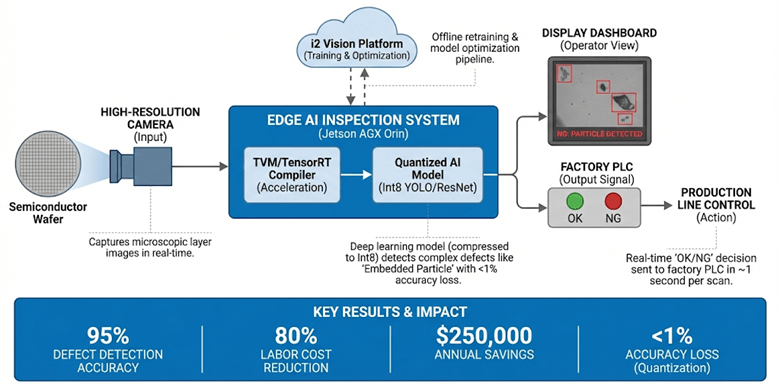
They partnered with Cardinal Peak/FPT Software to engineer a custom computer vision and edge AI solution. Leveraging the i2 Vision platform and deep expertise in model optimization, we deployed a system capable of detecting microscopic defects with 95% accuracy. Furthermore, our engineers optimized 11 distinct deep learning models for deployment on constrained edge devices, reducing inspection latency to under 1 second while maintaining precision.
The Challenge: The Limits of Manual Inspection at the Nanoscale
Semiconductor manufacturing involves layering microscopic circuits onto silicon wafers. NXP’s existing process required human operators to manually classify defects such as cracks, scratches, missing components, and edge chipping across individual layers.
This manual approach created three critical issues:
- Inconsistent Quality: Human fatigue led to missed defects (“escapes”) and false positives, impacting yield.
- Latency Bottlenecks: Manual review could not keep pace with the high-speed production line, creating a throughput cap.
- Deployment Constraints: The solution needed to run locally on the factory floor (Edge AI) to ensure data security and ultra-low latency, but standard AI models were too heavy for the available hardware.
In semiconductor manufacturing, manual inspection at the nanoscale is no longer a viable throughput strategy. By engineering a custom Edge AI pipeline that understands the visual ‘texture’ of microscopic flaws, we turned a labor-intensive bottleneck into a high-speed, 95% accurate automated optical inspection (AOI) solution.
The Engineering Solution: High-Performance Edge AI
We delivered an end-to-end automated visual inspection solution, moving from raw image acquisition to real-time “scrap” decisions at the edge.
Advanced Computer Vision with i2 Platform
Leveraging the i2 Vision accelerator (developed in partnership with Landing AI), we trained deep learning models to perform high-fidelity feature extraction to identify the visual ‘texture’ of microscopic flaws—distinguishing harmless dust from critical cracks, scratches, and embedded particles that rule-based systems miss. The system was trained to detect specific anomalies like “Large-area Surface Defects” contamination and “Embedded Particles” with high precision.
Edge AI Model Optimization & Benchmarking
To ensure the system could run on constrained edge hardware (ARM-based chips), our engineering team performed a rigorous optimization campaign.
- Model Selection: We characterized and benchmarked 11 different AI architectures, including YOLO (v3, v4, v5), ResNet50, MobileNet-v2, and EfficientNetV2, to find the perfect balance between accuracy and speed.
- Quantization: We utilized Post-Training Quantization (PTQ) and Quantization-Aware Training (QAT) to compress models from FP32 to Int8. This achieved a massive reduction in model size with less than 1% loss in accuracy.
Real-Time Inference Architecture
The final solution was deployed on Jetson AGX Orin edge devices. We engineered a full pipeline that integrated TVM compilers and TensorRT to accelerate inference, achieving a response time of approximately 1 second per scan.
Edge AI Inspection Architecture: Wafer Defect Classification
The Results: Precision at Scale
The transition to Custom Computer Vision & Edge AI Engineering transformed NXP’s quality control process:
- Under 1-Second Inspection Latency: Engineered a high-speed inference pipeline that keeps pace with the production line without a throughput cap.
- 95% Defect Detection Accuracy: The system reliably identifies microscopic flaws, significantly outperforming manual benchmarks.
- 80% Labor Cost Reduction: Automating the classification process allowed NXP to reallocate skilled technicians to higher-value tasks.
- $250,000 Annual Savings: Direct cost savings realized through reduced scrap and labor optimization.
- <1% Accuracy Loss: Our quantization engineering successfully compressed the models for edge deployment without compromising inspection quality.
The Engine Behind the Solution
This project was executed by utilizing our expertise in Edge AI, Hardware Engineering, and Computer Vision. Our ability to bridge the gap between heavy deep learning models and constrained hardware makes us the ideal partner for semiconductor and electronics manufacturers.
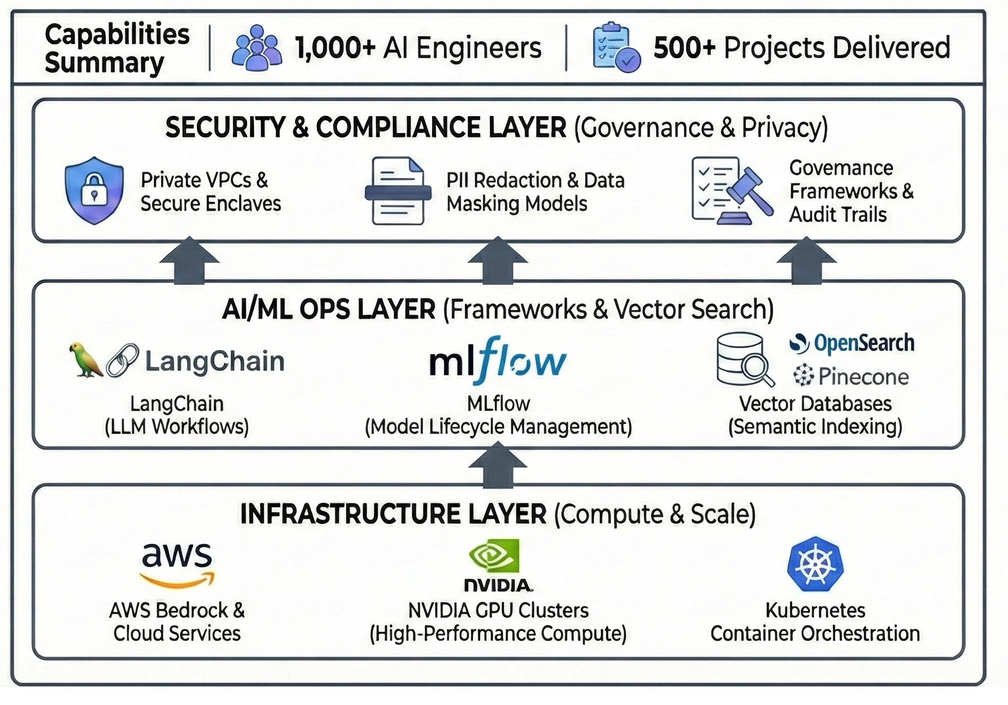
Our AI CoE Capabilities
Explore Related Computer Vision & Edge AI Solutions

Edge AI & Computer Vision Services
Discover how we optimize complex AI models to run on resource-constrained devices without sacrificing performance.
Visual Inspection Software Accelerator
Learn more about the i2 Vision platform and how it accelerates the deployment of automated quality control.


Custom Computer Vision & Edge AI Engineering FAQs
How do AI & Data Product Engineering Services improve semiconductor defect detection?
AI & Data Product Engineering Services replace rigid, rule-based machine vision with deep learning models capable of high-fidelity feature extraction. By implementing MLOps & Data Pipeline Engineering Services, we create a continuous feedback loop that allows models to distinguish between harmless dust and critical large-area surface defects with sub-second latency on the factory floor.
What are the benefits of Embedded AI Engineering Services for edge-based inspection?
Embedded AI Engineering Services enable complex computer vision models to run locally on constrained hardware like the NVIDIA Jetson AGX Orin. Through techniques like Int8 model quantization and TensorRT optimization, we ensure that high-precision inspection—detecting anomalies such as embedded particles—occurs in real-time without the latency or security risks of cloud-based processing.
What is Edge AI model quantization, and why does it matter?
Edge AI model optimization frequently utilizes quantization, an engineering process that reduces the numerical precision of an AI model (e.g., from FP32 to Int8) to make it smaller and faster. This is critical for Edge AI because it allows powerful models to run on small, power-efficient chips inside factory machines without needing a connection to the cloud.
How does this solution handle different types of defects?
We use deep learning for automated optical inspection (AOI). Unlike traditional systems that look for simple measurements, our models learn the visual “texture” of defects. This allows the system to distinguish between a harmless dust particle and a critical crack or scratch, drastically reducing false positives.
What is the ROI of AI-powered semiconductor defect classification?
ROI for AI-powered semiconductor defect classification is driven by three primary factors: an 80% reduction in labor costs by automating manual inspection, significantly reduced scrap material, and increased production throughput. In high-volume fabrication environments, these systems can generate over $250,000 in annual savings while maintaining a 95% defect detection accuracy.